Products
- Other PCB & PCBA[5]
- Double-Sided PCB[6]
- Single-Sided PCB[4]
- Rigid PCB[6]
- Multilayer PCB[6]
Contact Us
- Contact Person : Mr. Lei Willson
- Company Name : Wenzhou Walbond Electronic Co., Ltd.
- Tel : 86-577-88518333
- Fax : 86-577-88950316
- Address : Zhejiang,Wenzhou,A-1 site,Center Road,Sanxi Industry Park,Ouhai Economic Development Area
- Country/Region : China
- Zip : 325000
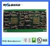
6 Layer Processors and Converters PCB with BGA


Product Detailed
Related Categories:Multilayer PCB
Related Product Searches:6 Layer Processors and Converters PCB with BGA,High Quality,Processors and Converters PCB,high tg 170 pcb,6L
1.6L cell phone PCB;
2.good quality,reasonable price;
3.quicker delivery;
4.better logistic service;
5.UL,SGS,ROHS,ISO
Related Product Searches:6 Layer Processors and Converters PCB with BGA,High Quality,Processors and Converters PCB,high tg 170 pcb,6L
We can manufacture PCBin higher quality, more competitive price, quicker delivery and better logistic service…Welcome to send us RFQ!
This form is of my company's process capacity for your reference, for more messages, pls contact with us freely!
| Item | Specification | ||
| Material | FR-4 / Hi-Tg FR-4 / Lead free Materials(RoHS Compliant)/CEM-3/CEM-1/Aluminium | ||
| Layer | single layer,double layer,multi-layer(4-10) | ||
| Board Thickness | 0.3mm-3.0mm,+/-0.1mm(tolerance) | ||
| Copper Thickness | 1/2OZ-3OZ (35um to 105um),+/-8um(tolerance),purity 99.5% | ||
| Impedance Control | ±10% | ||
| Bow and Twist MAX. | 0.75%(SMT) | ||
| Anti-strip | 0.88N/mm | ||
| Resistance | ≤20Ω | ||
| Reactance | 500V | ||
| Min. Value | |||
| Min. Trace/Space Width | 6 mil,+/-0.15mm(tolerance) | ||
| SMD Pitch | 10 mil | ||
| BGA Pitch | 20 mil | ||
| Min Pad Space | 4mil(SMT) | ||
| Plating Copper Thickness | 15um | ||
| Hole | |||
| Hole Size | 0.25mm--6.2mm | ||
| Hole Position Tolerance | ±0.1mm | ||
| PTH/NPTH Tolerance | ±0.15mm(dia.=0.4-1.4mm) | ||
| Pad Tolerance | ±0.1mm(dia.≥0.6mm) | ||
| Pad to hole/to pad Tolerance | ±0.05mm/±0.2mm | ||
| Solder Mask | |||
| Pad no Open | soldermask must cover all on both side, reject tin on pad | ||
| Pad Open | reject soldermask inside the hole on both side | ||
| Solder Mask Thickness | 0.7mil,raised H≤0.05 | ||
| Colour | green,blue,red,yellow,black,white(LPI/MATT.,UL 94 V0 approved) | ||
| Surface Finish | |||
| HAL | tin height≤0.05mm | ||
| ENIG | Nickel 3-7um,gold:0.5-0.7um | ||
| OSP/flash gold | 0.2-0.5um | ||
| Pealable mask | cover all on pad,thickness≥0.20mm | ||
| Carbon Ink | cover all on trace,Value≤30Ω | ||
| Outline | |||
| Outline Tolerance | ±0.2mm | ||
| Beveling | 30°,45° | ||
| V-cut position/depth | ±0.2mm(length≤100mm)/±0.2mm | ||
| Punch | ±0.1mm | ||
| E-testing pass percent | 97% pass for the first time,+/-2%(tolerance) | ||
| Certificate | SGS,ISO,ROHS,UL, | ||
Welcome to visitWALBOND !
6 Layer Processors and Converters PCB with BGA